Nanomaker (Software for nano/micro lithography )
This software package was developed by Interface Ltd. and can be used in microelectronics and nanotechnology industries and research centers for designing and manufacturing modern micro- and nanoelectronic devices.
Purposes:
1. To convert any scanning electron microscope (SEM) into an e-beam lithograph.
2. To obtain ultimate resolution during lithography resolution
for a certain setup. To this end:
3. To predict results of lithography by simulating.
4. To ensure adjustment for various configurations of lithographic
equipment; for the presence or absence of beam blanking systems, stages, etc.
5. To create three-dimensional structures in a resist.
6. To familiarize user with the basic principles of lithography.
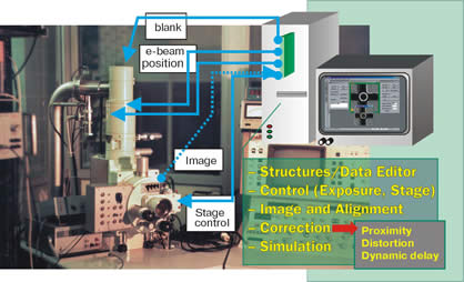
Picture 1. Scanning Electron Microscope controlled by the
software
Description
The software package was developed to perform three basic functions:
1. Data preparation for exposure ( via Graphical Data Base).
2. Exposure control
3. Video control, system tuning
Applications
Easy installed on:
System Requirements:
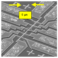
Picture 2
Alignment for successive e-beam and optical lithographies
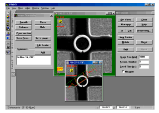
Picture 3
Operation with superconductive nanodevice, IMT
RAS (Russia)
Picture 4
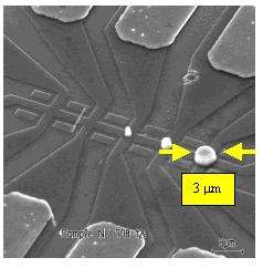
Microdevice on 2DEG for magnetic measurements
Picture 5
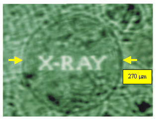
Image generated by X-ray Phase hologram made by e-beam lithography, Bessy II
(Germany), IMT RAS (Russia)
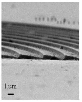
Picture 6
Kinoform optics by 3D lithography