3D DESIGN IN E-BEAM LITHOGRAPHY
V V Aristov, S V Dubonos, R Ya Dyachenko, B
N Gaifullin, V N Matveev, H Raith*,
A A Svintsov, S I Zaitsev
Institute of Microelectronics Technology,
Academy of Sciences,
Chernogolovka, Moscow district, 142432, Russia
e-mail: zaitsev@micro.ac.su
*Raith GmbH, Hauert 18, D-44227 Dortmund, Germany
Abstract A technology micro/nanostucturing based on e-beam lithography, plasmo-chemical etching and electrochemical deposition is developed. It allows to create structures in organic resist on substrate of predefined profile with vertical sizes in range 50nm-5um and 50nm-1mm in lateral direction (Fig.3). Metal replicas was created by electro-chemical deposition (Fig.4). The replicas were used then as a stamp for fast transferring of relief in soft material (polymer) (Fig.5).
We expect application in optoelectronics, optical processing, creation of zone plates and other diffractive optical elements (calculated holograms).
We submit a method for creation of structures with designed profile in a resist, first results on transferring a profile in a substrate and copying (printing) in soft material (polymers). By this way a designed profiles with vertical sizes in range 10nm-1000nm and with lateral sizes in range 10nm-1mm may be created.
Today there is an increasing demand for producing real three-dimensional structures, such as blazed gratings, Fresnel lenses, diffractive optical elements, computer generated holograms, lens arrays and etc. In these cases the total area has to be exposed with a continuously variable dose, which of course needs proximity correction as well - but this was not available up to now. All established methods for proximity correction aim to correct for two-dimensional structures. Most of them just take care for an absorbed dose of 100% inside the exposed structures not considering the dose distribution outside, which is below the 100% level. Characteristic sizes of the optical elements mentioned above belong to range 100nm-10um so proximity effect correction is a crucial point of the whole design and technological chain.
3D correction
The method of "Simple Compensation" introduced by ARISTOV et al [1] has been developed to a very powerful tool for correction and simulation of proximity effects [2,3,4] which led to the widely used software package "PROXY".
If we aassume as usual the proximity function I(x,y) consists of two Gaussians with convential parameters a b and h
If a structure Q is presented as a set of rectangles (polygons) Qi (Q=Q1+Q2+Q3+ ...) and absorbtion dose distribution D(x,y) is defined as D(x,y)=D0=100% inside structure Q and zero outside then the method of "Simple Compensation" for exposure T at point (x,y) may be written (in equivalent to [1] form)
![]()
An aim of the above correction procedure is to obtain D(x,y)=D0=100% inside structure Q and as less as possible outside.
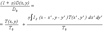
We extended this numerical calculation method for 3D correction [5], where each element of the exposed structure is assigned by a required (designed) absorbed dose D. Proximity 3D correction leads then to an exposure dose distribution T allowing to produce on all places the required absorbed dose. "3D correction" looks very similiar to the "simple compensation" and consists of sequantial steps. "3D correction" estableshes that dose is not constant inside structure but is actually spatially distributed D(x,y).
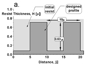
On practice we proceeded as following. Using graphical editor a stepwise relief was design, H(x,y) As an example (Fig.1a) consider a simple structure representing a phase graiting designed for polymer (PMMA) with refractive coefficient n=1.49. Then required absorbed dose D(x,y) just by considering the resist contrast was calculated (thick line on Fig.1b). After that an improved exposure time T1 was calculated
![]()
We used such a procedure in iteration.
![]()
...
![]()
5-10 iteration are sufficient to obtain self-consisted exposure time distribution T(x,y). On Fig.1b the final distribution of exposure dose T(x,y) after 3D correction is shown by thin line. It demonstrates nontrivial changes in compare with naive noncorrected distribution proportional to D(x,y).
Technological chain, examples and testing
"PROXY-WRITER" was used to expose all these irregular After exposure with T(x,y) and development we obtained as examples stairs, linear and circular zone plates with good reproducing of designed structure with up to ten levels in PMMA resist of micron thickness on Si wafer (Fig.3). As the next step we transferred the resist relief in rigid material by electro-chemical deposition of Cu (Ni) (Fig.4). The final step was mechanical printing in polymer material (Fig.5). Results of optical testing of created lenses showed focus spot about 5um with good efficiency.
Conclusion
1) V.V.Aristov, A.A.Svintsov, S.I.Zaitsev, Microelectronic
Engineering 11 (1990) 641-644
2) V.V.Aristov, B.N.Gaifullin, A.A.Svintsov, S.I.Zaitsev, R.R.Jede, H.F.Raith,
ME 17, 1992, p.413
3) V.V.Aristov, B.N.Gaifullin, A.A.Svintsov, S.I.Zaitsev, H.F.Raith and R.R.Jede,
J Vac. Sci. Technol. B 10(6), Nov/Dec 1992
4) S.V.Dubonos,B.N.Gaifullin,H.F.Raith,A.A.Svintsov,S.I.Zaitsev ME 21, 1993,
p.293
5) S.V.Dubonos,B.N.Gaifullin,H.F.Raith,A.A.Svintsov,S.I.Zaitsev Microelectronic
Engineering 27 (1995) 195-198.
 |
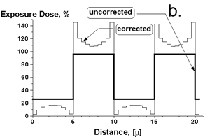 |
Fig.1 a. - A height of a designed simple grating should be of 0.63m (=l/(n-1)) to provide phase shift equal to p. b. - Even for a grating with period 10m the proximity correction (after PROXY) gives remarkable contribution and nontrivial distribution of exposure dose (substrate - Si, e-beam energy - 25KeV).
Fig.2. Technological chain apart from e-beam exposure with 3D correction, development includes electrochemical deposition of metal for obtaining rigid replicas, mechanical printing for producing copies from soft material.
3D NANO/MICRO-STRUCTURING FOR PRODUCING EFFECTIVE DIFFRACTIVE OPTICAL ELEMENTS
A A Aristov, S V Dubonos, R Ya Dyachenko, B
N Gaifullin, V N Matveev,
A A Svintsov, S I Zaitsev
Institute of Microelectronics Technology,
Academy of Sciences,
Chernogolovka, Moscow district, 142432, Russia.
e-mail: zaitsev@micro.ac.su
A new method for designing calculated holograms (diffractive optical elements) in form of a 4-levels relief is presented briefly. The calculation method is combined with earlier developed technological scheme based on 3D proximity correction, one step e-beam lithography and electroplating (for obtaining rigid stamp) to experimentally evaluate producing phase DOEs. Two demonstrators (passive splitter and generator of 3D scene) confirm reliability of the whole long set of design and technological steps.
|
Introduction These elements have several names kinoforms, diffractive optical elements (DOE), calculated holograms. The main feature of the elements is a continuous relief of a working layer. The advantages of diffractive optical elements are well known [1-5]. The main one is their higher effectiveness in comparison to binary (Fresnel) elements. An electron beam lithography was suggested in 1987 [1,2] for direct producing simple DOEs such as microlenses. An optical lithography was used for DOE producing together with replication by castings or embossing from a Ni shim [3]. The possibility of several sequential e-beam exposures (or several masks usage in photolithography) for continuous relief producing was analyzed and demonstrated in [4,5]. A technology of micro/nanostucturing is based on one-step e-beam lithography with 3D proximity correction [6, 7]. It allows one to create structures in organic resists (on a substrate) of the predefined profile with vertical sizes in the range 50nm-5um and 50nm-1mm in the lateral direction. Metal replicas were created by electro-chemical deposition from the resist profile [7]. The replicas were used then as a stamp for fast transferring of relief in soft material (polymer). By this procedure lenses of high efficiency were fabricated [7]. Plasma-chemical and ion etching were used to transfer the resist profile into Si and glass directly. |
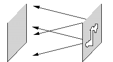
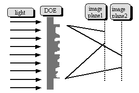
But the lens is a relatively simple element which transfers a parallel beam into a focal point. As to the generation of more complicated images, the fundamental problem is transferring of a parallel (or any given) beam into an arbitrary image. The key point of the problem is the fact that an experimentor (a technologist) is able to control the phase (or amplitude) only. It is not clear up to now whether it is possible or not to create arbitrary images manipulating by phase alone. The paper is devoted to an experimental evaluation of a new method for designing and creating an arbitrary image by DOE which comprises a four level hologram. The technological basis of the method is an electron beam lithography with nano/micro structuring. Experimental examples of DOE are presented. DOE design (hologram synthesis) A DOE design begins (Fig.1) with designing of an image (or even a 3D scene). The next procedure is calculating a field of a complex amplitude in the plane of the DOE (Fig. 2). It seems evident that if one is able to create an optical element by transferring an original wave front (for example a plane wave where the amplitude and phase are constant) into a wave with a calculated complex amplitude, the desirable image in the image plane |
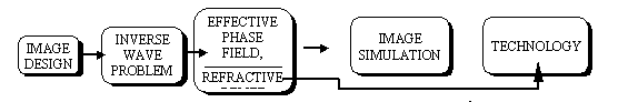
Fig. 1. DOE design steps include image (scene) design, hologram
(phase and relief) calculation and image simulation.
|
will be obtained owing to interference. But as was mentioned above, the possibilities to change simultaneously both the amplitude and phase we are restricted. Practically one can manipulate with a phase or with amplitude only. The technology [6,7] allows producing a given relief in a transparent material therefore we deal with the phase DOE. We developed a method of calculating an effective phase field from the complex amplitude. The method produces the phase field in form of a 4-level phase hologram. Details of the method including estimation of effectiveness of a 4-level hologram will be presented elsewhere. Of importance here is that the effective phase field is directly related to the relief via the refraction index of a DOE material. The analysis of relieves and our experimental experience show that the relief has spatial features with sizes from 100nm to 10um. This was the reason why e-beam lithography (not a photolithography) was used for DOE producing. in [4,5]. DOE technology The technology of DOE producing is described in [6,7]. The main advantage of the technology is the fact that only one e-beam exposure it used. This became possible after and due to the development of a special 3D proximity correction technique [6,7]. The possibility of the given relief creation was demonstrated by producing lenses with a continuous relief [6]. Further we developed additional technological steps to produce a rigid copy from the resist relief and to obtain copies of the relief from soft material [7]. We estimated the spatial resolution of the whole technological chain to be 50nm. This estimation was confirmed in [8] where resolution 25nm was achieved during imprinting in polymer (PMMA).
|
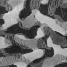
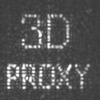
Two examples The first example (Fig.3) comprises a passive splitter of a parallel laser beam into tens of distinct beamlets. Fig. 2a shows a designed image where the beamlets are arranged as some letters. An effective 4-level phase field is shown in the gray scale in Fig. 3b. The hologram of 200um by 200um was calculate for PMMA with refractive index n=1.49 and for a laser with wave length l=632.8nm. An elementary height step provides the 3.14../4 phase shift. Figure 3c demonstrates a 200um by 200um lithographic pattern consisting of about ten thousand domains with specific exposure times assigned as result of the 3D proximity correction implemented in the advanced version of PROXY. We used the SEM JSM-840 as the exposure tool together with PROXY-WRITER for lithographic data preparation and exposure control. After the exposure and development 4-level relief in resist was created. Electroplating with Cu was used to obtain a rigid copy (a stamp) of the resist relief. The expected 4-levels of the metal are clearly seen in Fig. 3d. Several tens of polymer copies were than obtained by imprinting in heated PMMA. A PMMA relief of a polymer copy obtained by AFM is shown in Fig. 3e. The last picture Fig. 3f presents a computer simulation of an image corresponding to the 4-level DOE. image resulting from the 4-level hologram.
The sizes of the beamlets and their relative intensities for the image generated by real 4-level phase hologram were very close to those predicted by simulation. This was demonstrated during the paper presentation at MNE'96. The second example demonstrates the possibility to create not only image in the plane but 3D scene and comprises tens of focal spotlets concentrated in two distinct focal planes as shown in Fig. 4a. In this case a 200um by 200um hologram was created. Figure 4b and Fig 4c show the corresponding images in two focal planes. The sizes and relative intensities of the spotlets were consistent with the simulated picture. Conclusion A method for designing of calculated holograms (DOEs) in form of a 4-levels relief is presented briefly. The technological scheme based on 3D proximity correction, one step e-beam lithography and electroplating for obtaining rigid stamp for further producing cheap polymer copies of DOE is experimentally evaluated. Two demonstrators (passive splitter and generator of 3D scene) confirm the reliability of the whole long set of designing and technological steps. Reference 1.T.Shiono, K.Setsune, O.Yamazaki and K.Wasa.
J. Vac. Sci. Technol. B 5.33(1987) |
Micro- and Nano- E-Beam Lithography using PROXY
V.V.Aristov, B.N.Gaifullin, A.ASvintsov, S.I.Zaitsev, H.F.Raith*
Institute of Microelectronics Technology,
Chernogolovka, 142432, Russia
*Raith GmbH, D-4600 Dortmund
The PROXY software package was designed in the Institute of Microelectronics Technology in cooperation with Raith GmbH stands for a special attachment which enables any scanning electron microscope (SEM) to perform electron lithography. PROXY provides rapid and easy to operate pattern generation and writing on any substrate surface. The PROXY software package works on the IBM PC, and any compatible computer. It may be connected to various hardware components and includes mark recognition and control system for combining with motorized stage. Now, calculation of proximity correction, simulation of the results after development, distortion correction are possible in very easy and convenient way. By this way a correction procedure implemented in PROXY provides effective and automatic correction of proximity effect related with backscattered electrons and improves significantly proximity effects dealt with beam size resulting to a guaranteed accuracy about 40% of an electron beam radii.
INTRODUCTION
Large and sophisticated electron beam lithography instruments are a necessity in modern IC production - but besides this, there are many applications which need electron beam lithography at a much smaller scale. Some of these fields are: optimizing of electron resist, integrated optics experiments, X-ray optics with zone lenses, experiments with individually created IC components, window etching in ICs for failure analysis, epitactic and galvanic experiments. Main phenomenon restricting a resolution of e-beam lithography is so called proximity effect when backscatered electrons expose places far from inlet point of e-beam. A proximity distance depending on electron energy and substrate material belongs to micron (several microns) range. First attempts to correct proximity effect were made more than fifteen years ago [1,4,6]. Proximity correction means to calculate a required primary exposure dose in each point of structure in order to obtain an even absorbed dose inside all structures considering the contribution of backscattered electrons, beam size and forward scattering. Many studies have been done in this field, suggesting different correction methods. But no method allows to calculate a guaranteed final accuracy especially by taking into account the process of resist development, except the method of "simple compensation" which was introduced by Aristov et al [6,8]. Another process in e-beam lithography influencing on structure shape is development. Using models considered in [2,3] a fast and effective algorithm for development simulation was suggested. This work describes models of exposure and development, method of proximity correction and its accuracy. Allthis is a base of software package PROXY which enables any scanning electron microscope (SEM) to perform electron lithography
FORMULATION OF THE PROBLEM OF PROXIMITY EFFECT CORRECTION.
The general problem proximity correction can be defined as follows:
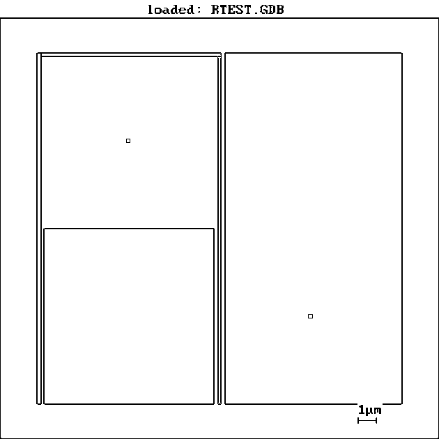
Given is a two-dimensional x,y structure consisting of non intersecting regions Qi , i=1,2,...,N, shown in Fig.1 by solid lines. Exposure doses are
![]()
After development during time t the resist projection onto the substrate surface (plane x,y) represents structure Q comprising the elements Q shown in Fig.1 by dotted lines. We suggest that the error d should be defined by the maximum distance between the boundaries of structures Q and Q.
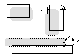
Fig.1
The problem of the correction is to find such distribution of exposure doses T(x,y) that after exposure and development the errors of the whole lithographic process d would be less than a prescribed or desirable value.
2. EXPOSURE AND DEVELOPMENT MODELS.
Absorbed dose distribution D(r), r=(x,y,z), in the resist depends linearly on exposure dose T(x,y). For correction it is generally assumed that D is independent on resist depth z [1] , which leads to
![]() D0
and T0 are absorption and exposure sensitivities of a resist respectively. The
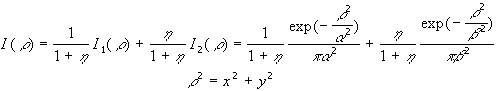
proximity function I(r), r=(x,y), is written as a sum of two Gaussians
D0
and T0 are absorption and exposure sensitivities of a resist respectively. The
proximity function I(r), r=(x,y), is written as a sum of two Gaussians
,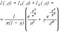
which are interpreted as contributions of primary beam, I1(?), and backscattered electrons, I2(?), Here I, I1 and I2 are normalized on unity. The primary beam is concentrated in the area of radius ? and the backscattered one in the area of radius ?, with ????. Factor ? characterizes the contribution of backscattered electrons to the exposure in a large area. ? and ? are the characteristic lengths of the exposure process.
We use Two Gaussian model due to several reasons. First, two contributions have clear physical meaning (primary electrons and backscattered ones). Second, experimental measurements and simulation of absorbed dose are described by Gaussian model very well [10]. And third, an appearance of the third Gaussian is dealt in our opinion with an influence of a development which usually is not taken into account in measurements of proximity function. In [11] was shown that considering development the third Gaussian disappeared.
An independence of proximity function I(r) on depth z is a good approximation due to the fact that the transport length of a resist for conventional in electron beam lithography energy normally is much more than resist thickness H . Therefore it is possible to neglect low-angle spreading of a primary beam. In any case below we assume the value of a beam size on interface of resist-substrate as upper estimation of ?.
Because ? is normally much smaller than ? and than the resist thickness H , it can be assumed (this is shown in [12]) that it causes an edge effect only, and therefore the correction can be done separately just inside a small structure frame in a secondary step.
Considering first the backscattering effect only (described by ? and ?), it is possible (according to the arguments of [8]) to substitute the first Gaussian by ?-function I. As a result if a structure Q is presented as a set of elements Qi (Q=Q1+Q2+Q3+ ...) and dose distribution D(x,y) is defined as D(x,y)=Do=100% inside structure Q and zero outside then the method of "simple compempenation" for exposure T in point (x,y) may be written (in equivalent to [6,8] form)
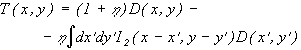 Pay
attention that only the second Gaussian, I2, corresponding to backscattered
electrons is used. In the formular exposures T and D are measured in percents
with T0 and D0 equal to 100%
Pay
attention that only the second Gaussian, I2, corresponding to backscattered
electrons is used. In the formular exposures T and D are measured in percents
with T0 and D0 equal to 100%
3. 3D-SIMULATION OF THE DEVELOPMENT
Liquid development of positive resists is adequately described by the model of isotropic local etching [2-4] (ILE-model) which assumes that the velocity of resist boundary movement is independent of the boundary form (locality of etching) and the direction of the boundary (isotropy of etching), but defined only by development rate V at the point which the boundary passes through at a given moment. Development rate V, in turn, is defined by absorbed dose distribution D and the dose characteristic of the resist written as [4]

where ? is the contrast of positive resist. A numerical method for development simulation is especially fast and effective for 2D case [2,3].
The development simulation is a convenient tool for research and industrial applications. For known T(x,y), I , and dose characteristic (?,D0 ), it is principally possible to calculate the resist profile at any moment during development, but practically this 3D problem is very difficult. To provide the possibility of development simulation after proximity correction the 2D-method for the 3D-case (V=V(x,y)) was extended. For this we use a set of cross-sections of the resist. Each cross-section has to contain a vector of rate gradient. In case of step function the latter means that the cross-section is perpendicular to the level contour. And now it is possible to solve the development problem of reduced dimensionality in each cross-section separately using 2D-algorithm mentioned above.
4. REALIZTION and examples
The procedures of proximity correction and development simulation comprise a kernal of a software package PROXY. Besides this it contains an efective tool for design of structures and additional option allowing to control exposure by SEM via a special hardware called patern generator.
In comparison to production beam lithography machines, the PROXY-SEM combination offers more flexibility in operation, more capabilities with respect to nanolitography, experimental electron beam lithography at a small fraction of the cost of currently available instrumentation. PROXY cannot be used as an IC production machine, however, PROXY offers much in fields of beam lithography research and development, especially since it is not limited to SEM's only, but to any other scanning system.
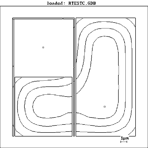
The first example is a structure which is not occasionally lookes like a field trnsistor (Fig.2) where parts A and C simulate source and drain, B is a gate, parts D and E are wires situated partly far from and partly very close to large pads. The original structure was designed by PROXY graphical editor, the gate B and two slots between gate and parts A,B were designed as 200nm. Consider a situation when each poinyt of the structure is exposed with exposure dose T equal to 150%. Development simulation (Fig.3) shows that due to proximity effect it is not possible to obtain the structure uniform exposure. Gate area is overexposed where as area D with single standing wire is underexposed. Fig.2b shows distribution of exposure time according to “simple compensation” generated by PROXY where as Fig.3b with simulation data predects promissing result. We carried out special experiments to check correction and simulation. We used JSM-840 as a lithograph under PROXY control for exposure the structures without correction and according to proximity corrected data. E-beam exposure and development of positive resist were followed by thin metal deposition and “lift off” operation so light image is Al layer. Comparison of simulated pictures with experimental ones show beautiful coinsidence which cofirms physical models of exposure and development, numerical algorithms and prosedures impementd in PROXY and correct operation of the system at whole.
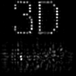
Next example demonstrates ultimate possibilities of e-beam exposure and comprises a world map written in an area of micron size (Fig.4). A STEM with very fine beam was used for direct writing using layer of aluminum fluoride.
More practical structure is shown on Fig.5, the structure was created for experiments with single electron transport.
References:
[1] M.Parikh IBM J. Res. Dev., 1980, v.24, N.4, p.438-451.
[2] S.I.Zaitsev, A.A.Svintsov, Poverkhnost',1986, N.4, p27-31.
[3] S.I.Zaitsev, A.A.Svintsov, Poverkhnost',1987, N.1, p47-52.
[4] A.R.Neureuther, D.F.Kyser, and C.H.Ting. IEEE Trans. Electron Devices 1979,ED-26,p.686.
[5] A.N.Broers, IBM J. Res. Develop. 1988 v.32, N 4, p.502-513
[6] V.V.Aristov, S.I.Zaitsev, A.A.Svintsov, Preprint, Chernogolovka, 1989
[7] S.V.Babin, A.A.Svintsov, Microelectronic,1989 v.18,N4, p.316-320
[8] V.V.Aristov, A.A.Svintsov, S.I.Zaitsev. Microelectronic Engineering 11 (1989)
641-644.
[9] Raith GmbH, product info PROXY, 1991
[10] U. Werner, F. Koch, G. Oelgart. J.Phys. D: Appl. Phys. (1988) v.21, p.
116-124.
[11] S. I. Babin, A.A. Svintsov. Microelectronic
Engineering 17 (1992) 417-420.
the absorbed dose distribution (2.1) will take the form
The previous general declarations will be illustrated in the report by set of examples. It includes: